| Home > Tutorials > Navigating FPGA Design |

Over the past 35 years, there has been a constant progression of technologies for performing digital signal processing. Some of these have been in the form of processors dedicated to the task of efficiently executing complex math in parallel such as Digital Signal Processors (DSPs) from Texas Instruments and Analog Devices and other specialized processors from other manufacturers.
Another path has been to exploit the specialized processing engines inside more general-purpose processors from companies like Intel and Motorola, or to re-purpose highly parallelized processors like Graphics Processing Units (GPU) for DSP applications like RADAR.
In each of these examples, it has been the software engineer's job to create programs or applications for a fixed hardware architecture. This might be accomplished by programing on the "bare metal" and accessing internal registers and resources of the processor directly, or through the window of an operating system that manages the processor's resources.
This paradigm changed with the introduction of programmable logic devices, and specifically with the advent of Field Programmable Gate Arrays (FPGAs). An FPGA's logic is a mesh of gates and interconnects that have no function until a logic design is loaded into the array connecting the gates to form circuits. Modern FPGAs can contain millions of logic gates and thousands of embedded DSP processors, allowing FPGA hardware designers to create extremely sophisticated and complex application-specific hardware functions. And this is where the job of the software engineer takes a turn.
With fixed targets like Texas Instruments DSPs or Intel processors, the software engineer writes programs for a static and well-defined hardware architecture. But with FPGAs, the functions and even the interfaces into the hardware are determined by which logic design the FPGA engineer uses to configure the FPGA, and this can change with different iterations of the design.
FPGA logic design and the software to control it are intimately tied together. This relationship, and the need to keep FPGA IP changes and software changes in sync, are a reality that must be managed in the design environment of sophisticated FPGA-based systems.
The increasing complexity of high-performance FPGAs has made the task of the FPGA designer increasingly demanding. The logic design, sometimes called Intellectual Property or IP, is typically created using VHDL or Verilog, which are hardware description languages for designing processing logic. Although these languages are the cornerstone of FPGA design, new tools and design environments can improve design efficiency, particularly when designing for very large FPGAs with millions of gates.
Pentek's new Navigator® Design Suite (see Figure 1) addresses these challenges with solutions for both FPGA and software engineers. The Navigator Design Suite was designed from the ground up to work with Pentek's new Jade™ architecture products and provides an unparalleled plug-and-play solution to the complex task of IP and control software creation and compatibility.
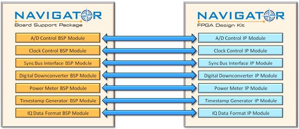
The Navigator Design Suite contains two separate but closely related products: the Navigator™ FPGA Design Kit (FDK) for integrating custom IP into Pentek-sourced designs and the Navigator™ Board Support Package (BSP) for creating host applications. Users are able to work efficiently at the API level for software development and with an intuitive graphical interface for IP design. Let's look at two design scenarios and how the Navigator Design Suite can be used in each.
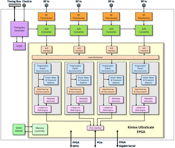
Found at the center of every Pentek data acquisition and processing hardware product is an FPGA. Pentek's new Jade™ family uses a Xilinx® Kintex® Ultrascale® FPGA. Like all Pentek products, Jade includes a full suite of built-in FPGA based functions (see Figure 2). In the case of an A/D converter product, these functions include:
In many cases, users will find that the built-in functions satisfy all the requirements of their application and no custom FPGA IP is needed. For these users, the FPGA looks like just another piece of hardware with fixed functions and a fixed interface for status and control.

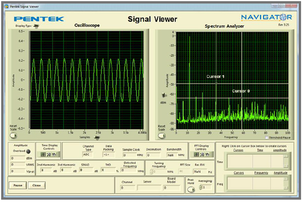
In this situation, the Navigator BSP API is the best solution for creating applications that control the Jade hardware. Provided as a C-callable high-level API, many of the most commonly used built-in functions can be controlled with simple commands. In addition, example programs and the included Signal Viewer (see Figure 3) allow users to immediately start acquiring and displaying data in the time and frequency domains without the need for creating any code.
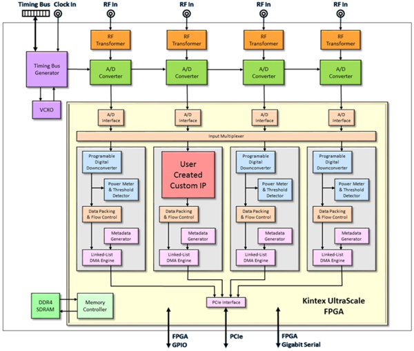
But what if an application requires special processing that only custom IP can provide? (See Figure 4). The solution is the Navigator FDK. It was created to work directly with the Xilinx Vivado® Design
Suite and creates a seamless environment for developing IP on Pentek products. The Navigator FDK leverages two new features in Vivado to greatly streamline IP development: the AXI4 standard and the IP Integrator.
AXI4 is the 4th generation of an interface specification from ARM® commonly used in the semiconductor industry. Xilinx has adopted this standard to create AXI4-compliant plug-and-play IP. The benefits can be seen immediately:
Navigator FDK follows the AXI4 standard. For Pentek's Jade data acquisition and processing products, the FDK includes the complete IP that is factoryinstalled in the board. This includes all interface, processing, data formatting, DMA functions, etc. IP designers can modify or replace functions as needed to match application requirements, and will find immediate compatibility with Xilinx IP and third-party IP that uses AXI4. Designers who create their own custom IP using the AXI4 standard will find integration with the Pentek-supplied IP straight-forward.
So how is the FPGA design actually edited? This is where Navigator FDK exploits another new feature of Vivado: the IP Integrator (see Figure 5). The concept of creating FPGA designs by connecting blocks in a graphical interface, similar to drawing a schematic, is not new, but Xilinx's IP Integrator makes it a practical solution.
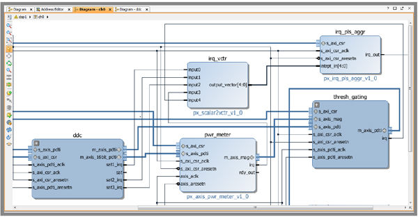
To edit a Pentek product design, an FPGA engineer opens the Navigator FDK design in Vivado. He then has immediate access to the entire board design as a block diagram. Individual IP cores can be removed, modified, or replaced with custom IP to meet the application's processing requirements. Because all blocks have AXI4 interfaces, connections between blocks can simply be "drawn" with wires or buses and the AXI4 interface handles the "housekeeping" of different bus speeds or widths.
Viewing an FPGA design as a block diagram enables the designer to see the data flow and simplifies the design processes by working at the "interface" and not the "signal" level. If, at any time, a designer needs to work with the VHDL code directly, it is always accessible in a source window, as well as full on-line documentation for every Pentek IP core.
Once a board's function has been modified by changing FPGA IP, it is most likely that changes will need to be made in the software controlling the board to support the new function (see Figure 4). While the Navigator's API is ideal for creating applications for the board, it assumes the board functions have not changed from the factory-installed set.
Once custom IP is introduced in the FPGA, the Navigator BSP module library is the solution for modifying or creating new software. Designed to work with the Navigator FDK, the Navigator BSP is structured to simplify this process. Each Navigator IP core module found in the FDK has an equivalent software module with a similar name in the Navigator BSP (see Figure 1). Changes made to an IP module can be easily traced back to the BSP module to make the necessary changes to control the new IP. This one-to-one relationship between IP and software greatly simplifies the task of keeping IP and software in sync.
The Navigator FDK's plug-and-play compatibility depends on IP cores following the industry standard AXI4 interface specification. A great place to start learning more about AXI4, Xilinx's IP Integrator, and Pentek's Navigator FDK is the Navigator IP Core Tutorial. This 100-page guide introduces the AXI4 interface and how it's used in Navigator and IP design. It also includes a complete learning lab to follow in Vivado that shows how to create a new core that is immediately compatible with Xilinx and Pentek IP.
| CONNECT ON SOCIAL: |
|
|
|
|