| Home > Tutorials > Advances in CPUs, FPGAs, and SoC Technology |

In almost every aspect, CPUs and FPGAs are radically different devices. And yet, they often compete for some of the same embedded system tasks. Choosing the best approach depends not only on the capabilities of each device, but also on the often disparate expertise of engineers promoting their respective development methodologies.
To make matters even more complicated, SoC (system-on-chip) technology now combines CPUs and FPGAs within the same device. Here, efficient interoperability becomes essential to meet stringent realtime performance levels. This article presents these challenges along with some strategies for developing successful solutions.
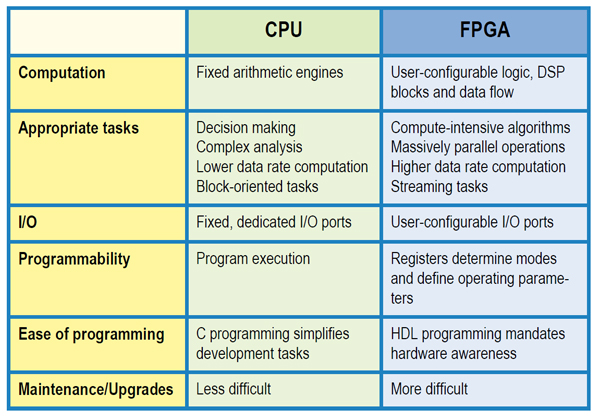
FPGAs are user-configurable hardware logic, while CPUs are fixed arithmetic engines executing user programs. Table 1, below, shows how these considerable differences translate into application tasks and implementation.
One of the latest CPU processor cores, the ARM Cortex-A72, sports up to four 64-bit ARMv8-A processor cores operating at clock rates up to 2.5 GHz. It targets powersensitive, high-performance mobile applications, and features a NEON 128-bit SIMD engine for efficient fixed- and floating-point vector processing. Interfaces to other processors and external memory are based on AMBA, discussed later.
The latest FPGAs from Xilinx, such as the UltraScale+, provide over 11,000 DSP engines, the essential building blocks for signal processing algorithms. They are aimed at high-performance embedded computing requirements with configurable interfaces for exotic peripherals and standard resources like DDR4 memory, PCIe Gen 4, and 100 GbE.
These differences drive the typical task assignments shown in Table 1. The complex aspects of high level decisions and data analysis are usually easier to implement in a CPU. Compute-intensive signal processing or data crunching tasks can take excellent advantage of the numerous DSP blocks found in FPGAs. Common examples, such as FFTs, matrix processing, and digital filtering can exploit the benefits of thousands of DSP blocks operating in parallel. Furthermore, FPGA hardware surrounding these blocks can be tailored for each application. This includes local data buffers, specialized FIFOs, and optimized interfaces to and from external sensors, storage devices, networks, and system components.
Choosing between an FPGA and a CPU for a given function is sometimes obvious because of its nature, but other times it could go either way. If so, the deciding vote is often cast for the CPU because a C program is easier to develop, maintain and upgrade. Another important factor: it is often easier to hire a C programmer than an FPGA design engineer!
In spite of their profound differences, CPUs and FPGAs have each staked out roles as essential elements in embedded systems.
Recognizing this symbiotic relationship, many vendors now offer SoC (system-on-chip) devices combining CPUs and FPGAs in a single monolithic silicon device. It is important to note that "SoC" also refers to highly-integrated devices that include analog interfaces, video and network ports, human interfaces, as well as RF and wireless interfaces, but not necessarily FPGAs. These SoCs are used extensively for consumer market products such as vehicles, smart phones, tablets, appliances, printers, and entertainment systems.
But to address the toughest requirements, real-time embedded systems often need a much narrower class of SoCs with the extra horsepower of large FPGAs. Leading the industry for such SoCs are Xilinx and Altera.
Xilinx offers the Zynq family of SoCs that combine ARM processors with Xilinx FPGAs. Their latest offering is the Zynq UltraScale+ series, whose processing section includes a Quad-Core ARM Cortex-A53 application processor, a Dual-Core ARM Cortex-R5 real-time processor, and a Mali GPU (graphical processing unit). To match a wide range of embedded applications, the programmable logic section includes a different mix of 16 nm FPGA resources in each of the eleven members of the series. With almost a million logic cells and over 3,500 DSP slices, they deliver significant computational power.
Altera competes with the Stratix 10 family of SoC devices, also using the Quad-Core ARM Cortex-A53 CPU. Altera's latest 14 nm FPGA technology offers ten different resource-balanced versions, one topping the list with over 5 million logic cells and 5,760 DSP blocks. Unlike Xilinx's counterpart, the DSP blocks of Stratix 10 can handle not only single- and double-precision fixed point operations, but also single-precision IEEE 754 floating point functions. This allows designers to achieve a much higher dynamic range for sensitive signal processing applications, and saves the often tedious task of optimizing scaling to avoid saturation and underflow conditions which can often plague fixed point hardware.
Because of parallel hardware structures connected directly to I/O ports, FPGAs can process and deliver high-rate continuous streaming data. CPUs are much more effective when processing data blocks in system memory. The advent of SoCs has thus created fundamental interface and data flow inconsistencies between FPGAs and CPUs.
To help resolve this challenge, ARM, Ltd. developed the Advanced Microcontroller Bus Architecture or AMBA nearly two decades ago. Since then, it has been widely adopted as an open source, welldocumented, license-free interface protocol between CPUs and peripherals, including FPGAs.
One of the most prevalent versions of AMBA is the AXI4 (Advanced eXtensible Interface Rev 4) specification. It presents a comprehensive standard for transferring data between master and slave devices for data widths from 32 to 1024 bits in burst lengths of 1 to 16. A master and a slave device, both having AXI4 compliant interfaces can be connected together and communicate, regardless of the nature or function of the devices.
Another popular variation is the AXI4-Lite specification, a subset of AXI4 for very simple devices that may not need the extra interface overhead required for full AXI4. Here, the data width is only 32 or 64 bits and the burst length is limited to single transfers. This is ideal for reading and writing to memory-mapped status and control registers, often satisfying the needs of most small peripheral devices.
Yet another derivative is the AXI4-Stream specification, which eliminates the addressing of AXI4 and AXI4-Lite. Instead, data bytes can be organized in packets of convenient size, and packets can be combined into frames tailored to a wide range of applications like specialized video and imaging. Each byte can be a data byte, a position byte to mark relative location of data bytes, or a null byte to serve as a filler. AXI4-Stream supports only unidirectional transfers from the master device to the slave device.
One important aspect for all of these AXI4 specifications is the concept of "interconnects". An interconnect is circuitry that joins one or more master interfaces to one or more slave interfaces, providing not only the required data path connectivity, but also adjusting the required data width and clocking for all devices. Nevertheless, if a single master needs to connect to a single slave, and the data widths and clocks are the same, they can be connected directly without the interconnect.
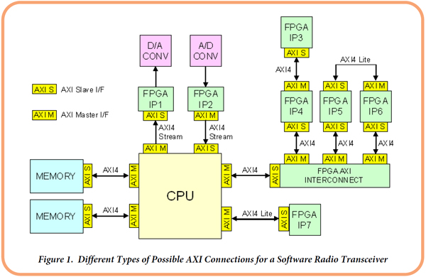
Figure 1 shows how AXI4 interfaces connect some typical blocks of a software radio transceiver. Note examples of AXI4-Stream for the A/D and D/A converters, and the AXI4-Lite for a simple FPGA peripheral in IP7. The AXI interconnect contains the FPGA logic that allows the CPU to access three IP blocks. Direct AXI4 connections between two IP blocks are possible when the clocking and data widths match.
AXI4 makes life much easier for SoC developers by supporting connections among a diverse range of components through a common interface standard, with interconnect blocks to realize system topology and reconcile data widths.
Another important point is that AXI4 can be extremely effective in reducing power and boosting transfer rates compared to competing strategies. This is extremely important for high-performance FPGAs in real-time embedded computing systems.
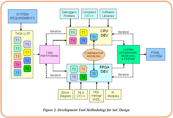
For all of these obvious benefits, both Altera and Xilinx have harnessed AXI technology for their latest development tool suites, not only for SoC development but even for IP in processor-less FPGAs. Figure 2 illustrates the development tool methodology for SoC design. Tasks are created to satisfy system requirements, and then initially partitioned as candidates for execution by either the CPU or the FPGA. During the development and modeling of each task, it may become apparent that a task may need to be reassigned to the other resource. Additional reassignment or optimization may occur when CPU and FPGA tasks are combined and tested during system integration.
Xilinx's SDSoC Development Environment supports their Zynq SoC devices. Familiar C/C++ design inputs to Eclipse compiler tools help developers determine which tasks dominate the CPU workload. Such tasks might be shifted to the FPGA programmable logic to help achieve the required real-time performance. SDSoC coordinates execution of both the CPU and FPGA tasks, showing the effects of different partitioning and implementations of tasks within each partition.
Tasks assigned to the FPGA are directed towards the Vivado Design Suite, which uses HLS (high level synthesis) to create IP from the C/C++ design input. Alternative design input choices include HDL using Verilog or VHDL and block diagram tools like MATLAB using System Generator. In addition, the Vivado IP Catalog is an extensive collection of plug-andplay IP modules for signal processing, communication, imaging, matrix processing, data manipulation, coding and formatting. Third-party IP and RTL design entries can be turned into compatible IP modules using the Vivado IP Packager.
Regardless of the Vivado design input, all of these newly-created IP modules use AXI4 interfaces compatible with the existing IP Catalog modules. Vivado IP Integrator streamlines the installation of AXI4 interconnects as required to ensure interoperability between IP modules. SDSoC helps link these AXI4 interfaces to compatible AXI4 links on the ARM CPU. The SDSoC and Vivado thus produce a fully synthesized modular SoC design complete with memory mapping, modeling, debugging tools, test benches, and timing analysis.
Altera's SoC Embedded Design Suite includes the Altera edition of the ARM DS-5 Development Studio to support the ARM CPU on Arria and Stratix SoCs. Based on Eclipse Tools, this open source extensible development environment includes compiler, debugger, and execution tracer.
Altera's QSYS System Integration Tool supports FPGA development tasks by graphically connecting IP modules from Altera and IP partners. Because they are equipped with AXI4 interfaces, QSYS automatically configures the required interconnects to implement the subsystem. QSYS creates custom IP using schematic or HDL design inputs.
Quartus II System Level Software integrates the Embedded Design Suite with QSYS for a complete development environment. It includes Altera's IP modules, and resources for modeling, analyzing, and debugging the interaction between the ARM CPU and FPGA resources. It optionally includes DSP Builder and support for OpenCL.
It is clear that both Xilinx and Altera are competing directly for high-end SoC designs by offering powerful ARM CPUs tightly coupled to powerful FPGAs, not only at the device level, but also with comprehensive and ambitious design tool suites. In fact, system integrators may be tempted to choose the SoC vendor based upon the effectiveness of the tools, more so than on silicon features. But switching SoC vendors is a major commitment for any company, and the potential benefits must be carefully weighed. Acquiring the training, skills, design methodology, expertise, culture, and effective points of contact for support from a new vendor is often decided only at the highest levels of corporate management.
Since we are still in the early days of SoC offerings, embedded systems developers can expect significant advances in performance over the next few years as vendors continue to boost silicon resources and race to provide tools to most easily take advantage of them.
| CONNECT ON SOCIAL: |
|
|
|
|