| Home > Tutorials > Board-Level Design Challenges for Military Software Radios |

Designers of mil-aero software radio boards must ensure outstanding signal quality and reliability across a diverse range of harsh operating environments. Size constraints and high component density require clever solutions for thermal management, shielding, filtering, noise reduction, power dissipation, and mechanical layout. Designers deal with these challenges using strategies developed only by tackling each issue, often through trial and error.
Modern radar and communication systems use wideband signals for improved range, resolution, and information content. Since virtually all of these systems now exploit DSP for maximum performance, the radio signals must first be digitized using high-speed A/D converters. Capable of operating at sampling rates of 5 GHz and above, they can deliver a single stream representing up to 2 GHz of bandwidth, avoiding the cumbersome band-splitting strategies previously required.
Unlike pure analog RF circuitry, which can be shielded in metal compartments, A/D converters present an existential confluence of analog and digital domains. Clock and data lines of an A/D can radiate spurious signals that contaminate its analog input, thereby reducing dynamic range and limiting system performance.
High-power digital circuits like FPGAs act as powerful RF transmitters, broadcasting energy through thousands of I/O pins. On-board switching power supplies, delivering up to 30 amps of current, operate at frequencies well within the input signal band. Making matters worse, small embedded system modules like XMCs must be densely populated, forcing close proximity of data converters, FPGAs, memories, power converters, and data buffers.
Maintaining analog signal purity requires extreme care in component placement, signal routing, shielding, isolation, as well as scrupulous power supply regulation, bypassing and filtering. Power and ground planes are perforated by thousands of vias, thus compromising their integrity and effectiveness. Fully automated routing often yields a trace pattern that makes the right connections but fatally corrupts critical analog signals.
A successful strategy usually requires human component placement and manual analog signal layout, followed by carefully guided semi-automatic routing of the digital signals. The final design requires inspection of each layer by an experienced engineer. Even so, hidden problems may not be resolved without two or more cycles of revisions and testing of the finished product.
During the last five years, software radio components have shifted heavily from parallel buses to multi-gigabit serial interconnections. Unlike traditional parallel bus backplanes, virtually all new embedded systems use serial links between boards and modules as evidenced by the shift from VMEbus to VPX.
The parallel LVDS data lines of data converter devices are also now being replaced by JESD204B serial links, taking full advantage of the rich complement of serial interfaces on the latest FPGAs and ASICs. This reduces power dissipation, offers scalability to higher rates, and dramatically drops the number of wires between devices by a factor of 8 or more. Operating at serial rates of 3.125, 6.25 and 12.5 Gbits/sec, JESD204B also supports lane bonding so that multiple serial lines can be aggregated to boost transfer rates.
Traditional DDR memories with parallel address and data buses are making way for a radically new memory called the Hybrid Memory Cube (HMC). It uses serial packets for reading and writing into vertical regions of stacked memory planes. Each packet contains a header with address and control information along with space for payload data. Featuring up to four access ports, each HMC holds up to 8 GB of data and supports read/write bandwidths as high as 320 GB/sec.
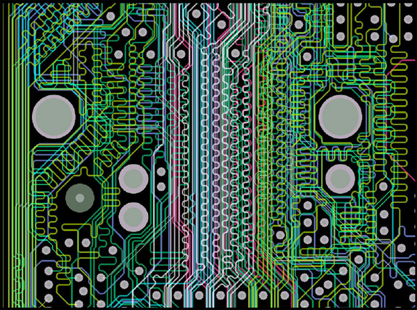
Reaping the many benefits of serial links forces circuit board designers to obey more stringent layout rules. Each serial lane uses two wires as a differential pair, which must be carefully matched in length to maintain signal integrity, often to within a few mils. The routing path of the pair may curve, adding extra length to the outside trace. Automated routing tools can compensate by adding extra loops and curves to undo the length discrepancies as shown in Figure 1. Additionally, bonded (multiple) lane interfaces like those between an A/D and an FPGA must maintain a common length across all lanes.
Other pitfalls for serial link circuit board design are impedance discontinuities along the traces, causing degraded transmission as the serial bit rate increases. Especially problematic are vias, connectors, stubs and pads. Running serial lanes across two different ground planes must be avoided, and special attention must be paid to the dielectric characteristics of the circuit board. Even the weave pattern of the laminate can distort the co-planarity of the traces, limiting the maximum usable bit rate. These effects can be modeled to a certain extent, but often the design can be fully validated only by product testing.
Although shrinking silicon process geometry helps reduce power dissipation for a given function, it also means more functions per package. As a result, next generation devices dissipate about the same total power as the previous generation, and removing this heat is a critical part of any system design. Some board vendors merely place components on a circuit board, and leave the thermal management task to their customers as part of system integration. This approach often requires expensive last-minute remedies that usually increase development costs and extend delivery times.
Conduction cooling techniques were first developed for older device packaging with through-hole pins that transferred heat to internal copper planes of the circuit board. Compression clamps along the edges of the board drew heat into metal card guide channels of the chassis.
Today, virtually all high power devices use ball grid array packaging, where most of the heat is delivered to the top surface of the package, exactly opposite of those early components. Now, the most popular strategy is a metal plate extending across the board, making thermal contact with all of the lids of hot devices, and bringing the heat to the metal side channels with clamps along the edges. Unfortunately, these metal plates must accommodate a wide variety of components, each with different heights and shapes. This mandates a custom plate uniquely milled with recesses for each device. To ensure good thermal transfer, conductive compound heat pads are installed on top of each device, conforming to fill the recess in the plate.
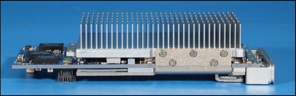
Forced air cooling is often more challenging due the number of variables. PCbased systems present an infinite combination of PCIe slot positions, fan types and placement, ventilation hole patterns, drive bay location, and power supply configuration. When necessary, creative heat sink designs can pull heat from high-power components like FPGAs around to the opposite side of the board where fins can engage with much more effective airflow, as shown in Figure 3. Fortunately, military radios usually use open architecture chassis like VME, VPX, CompactPCI, or MicroTCA, all of which offer more dependable airflow streams.
Attaching a mezzanine module to a carrier board presents yet a different problem. For example, most XMC modules have FPGAs on the same surface that faces the component side of a SBC carrier board, often sporting large processors. Not only are two high-power devices now radiating heat into each other, but the air space between the boards is greatly reduced. Often the best solution is a custom metal plate between the XMC module and carrier board that conforms to the top lids of hot devices on both boards. This alone is extremely effective for conduction-cooled systems. For air-cooled systems, the metal plate can also incorporate fins around the sides of the XMC module to access suitable airflow.
Responsible board vendors include temperature sensors at critical points around the board to help evaluate the effectiveness of thermal management strategies for each type of chassis. Thresholds can be set to automatically generate an interrupt to the host CPU for out-oflimit conditions. This facility can be incorporated in the operational software to serve as a useful health monitoring facility for deployed systems.
Other requirements like shock, vibration, altitude, humidity, EMI radiation and susceptibility, and environmental threats like salt, sand, and dust may require extreme measures, depending on the limits. If even only one of these factors is not properly addressed, the radio system can fail, possibly jeopardizing a mission or even the war fighter himself. While thorough product testing is essential, the integrity and reliability of any system must be designed in from the beginning, using guidance and practices best gained through experience.
| CONNECT ON SOCIAL: |
|
|
|
|