3
Pentek Homepage
Follow Us On LinkedIn Follow Us On Twitter Follow Us On YouTube Follow Us On Facebook Login AccountSign In
Board Selector   |  Recorder Selector   |  
Search:  
Home > Products > Model 78891

Your Pentek With YourPentek, you can be notified when new documentation and other updated product information is available for the Model 78891. Please login or register to manage your profile.

Model 78891 L-Band RF Tuner and 2-Channel 400 MHz A/D with Kintex UltraScale FPGA - PCIe

Request a Quote

Block Diagram

Datasheet

Manuals

Software

Development Systems

Literature

Life Cycle Management

Ordering & Warranty

Catalogs

Free Lifetime Support

 
  • Accepts RF signals from 925 MHz to 2175 MHz
  • Programmable LNA handles L-Band input signal levels from -50 dBm to + 10 dBm
  • Programmable analog downconverter provides IF or I+Q baseband signals at frequencies up to 123 MHz
  • Two 400 MHz 12-bit A/Ds digitize IF or I+Q signals synchronously
  • Two FPGA-based multiband DDCs (digital downconverters)
  • Xilinx® Kintex® UltraScale™ FPGA
  • Five GB of DDR4 SDRAM
  • Sample clock synchronization to an external system reference
  • PCI Express interface (Gen. 1, 2 & 3) up to x8
  • Clock/sync bus for multimodule synchronization
  • Optional LVDS and gigabit serial connections for FPGA for custom I/O
  • Optional optical interface for data streaming
  • Navigator BSP® for software development
  • Navigator FDK® for custom IP development
  • Spark® fully-integrated development system
  • Free lifetime applications support


Request a Quote

Model 78891

Jade Xilinx Kintex UltraScale FPGA Family Brochure
Jade Xilinx UltraScale
 

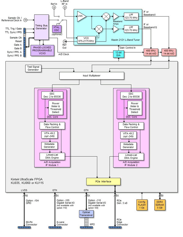
Model 78891 Block Diagram

Please refer to the product datasheet for a larger version of the block diagram


Hardware and Software Manuals - ( top )

Please note that some hardware and software manuals are used for more than one Pentek product. Although the model numbers given in the description of each manual below may vary, these manuals are all used for the product described on this web page.

A complete set of user manuals is provided in HTML format. Access to detailed documentation of the IP Core modules and their programmable registers is only available in the HTML version of the operating manual. Instructions for getting the HTML version of the user manuals is provided in the User Manual Library document listed below.

Part No.
Type
Description
Revision/Date
800.48145 User's Guide Navigator BSP for Jade User's Guide - Windows & Linux 4.2 (9/29/2023)
Contact Pentek
For Manual
Model 4811 Navigator FDK (FPGA Design Kit) for Model 78891

Software Products - ( top )

Model
Option
Description
4811 891 Navigator FDK (FPGA Design Kit)
4814 891 Navigator BSP (Board Support Package) for Linux
4815 891 Navigator BSP (Board Support Package) for Windows


CONNECT ON SOCIAL:  Follow Us On Facebook Follow Us On LinkedIn Follow Us On Twitter Follow Us On YouTube

Pentek, Inc. • One Park Way, Upper Saddle River, NJ, 07458, USA
Tel: +1 (201) 818-5900 • Fax: +1 (201) 818-5904 • Map + Directions • Site Map
Terms of Use • Privacy Policy • Copyright © 2024 Pentek, Inc. All Rights Reserved.