- PRODUCTS
- RECORDERS
- SUPPORT
| Home > Pipeline Newsletters > 8-Channel OpenVPX Beamforming System |
 | ||||||
|
Spring 2011 Vol. 20, No. 1 | ||||||
|
8-Channel OpenVPX Beamforming System Beamforming is a signal processing technique that utilizes an array of sensors to achieve directionality, increase the strength of transmitted signals and improve the quality of received signals. Beamforming is extensively used in communications, radar, direction finding, countermeasures, weapons systems, oil and mineral exploration, and medical imaging and treatment. Examples of software radio applications that use beamforming include direction finding. Here, the beamformed antenna can be steered to locate the arrival angle of a signal source. Two or more arrays can be used to triangulate the exact location of the source. This is essential for many signal intelligence and counter terrorism efforts. Principles of BeamformingBeamforming is typically used with an array of sensors or antennas to improve receptivity in a specific direction, for example, from a single cell phone as shown in Figure 1. The signal from a given source arrives at each antenna based on the distance between the source and the antenna, so the antenna signals have relative phase and amplitude offsets. 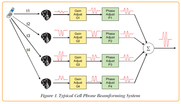 The beamforming process adjusts the gain and phase of each antenna signal to compensate for the different delays and signal paths. These adjustments align signals at each antenna for signals arriving from one particular direction. When the signals are summed together, the nonaligned signals arriving from other directions cancel each other while the signals from the beamformed direction add constructively for greatly improved signal-to-noise ratio. In this way, by electronically adjusting the gain and phase in each path, the antenna is effectively steered for directionality. System Block DiagramIn this system, eight antennas are arranged in a linear array, and the overall block diagram is shown in Figure 2 on the next page. The antenna frequency is 2.5 GHz, so each antenna signal needs to be amplified, filtered and then downconverted to an IF frequency so it can be digitized by an A/D converter. Synchronous sampling across all eight channels is mandatory to preserve a fixed phase relationship for beamforming. Samples from each A/D are downconverted to baseband complex I+Q signals in a DDC (digital downconverter), which also includes channel-specific phase and gain adjustments for the beamforming "weights". All eight baseband signals are then added together in summation blocks to produce the final beamformed sum signal. A CPU analyzes the sum and makes adjustments to the phase and gain coefficients to track or adapt to new targets. 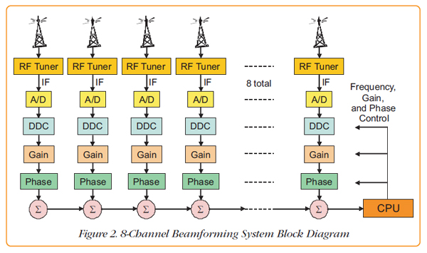 Model 53661 Beamforming BoardThe Model 53661 Software Radio board is a 3U OpenVPX Cobalt® board shown in the simplified block diagram of Figure 3. It features four 200 MHz 16-bit A/D converters, a timing, clock and synchronization section, and a Xilinx Virtex-6 FPGA. installed in the FPGA, are four DDC IP cores, each capable of accepting A/D samples from any of the four A/Ds. Each DDC has a decimation range of 2 to 64K and can deliver downconverted baseband bandwidths from 2.5 kHz to 80 MHz. Each DDC has programmable gain and phase shift controls accessible to the processor across the VPX backplane. In this system we will be assigning one A/D to each DDC. 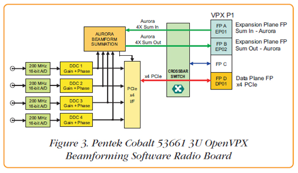 At the output of each DDC is a power meter (not shown) that calculates the downconverted signal power. Each power meter is equipped with a threshold detector that generates a system interrupt if the output power exceeds the upper threshold or falls below the lower threshold. These features simplify gain calibration and signal monitoring tasks that otherwise would have to be done in software by the system processor. The 53661 FPGA also includes an Aurora summation block that adds the four DDC outputs together to perform the channel combining for beamforming. Aurora is a lightweight link-layer gigabit serial protocol for Xilinx FPGAs. In this board, the Aurora interface accepts a propagated sum on one 4X input port and delivers the new propagated sum on a 4X output port including the contributions from the four onboard channels. Operating at a bit rate of 3.125 Gbits/sec, each 4X link can transfer data at 1.25 GBytes/sec.
8-Channel 3U OpenVPX SystemThe complete 8-channel OpenVPX beamforming system is shown in Figure 5. Two Model 53661 boards are installed in slots 1 and 2 of an OpenVPX backplane, along with a CPU board in slot 3. Eight dipole antennas designed for receiving 2.5 GHz signals feed RF Tuners containing low noise amplifiers, local oscillators and mixers. The RF Tuners translate the 2.5 GHz antenna frequency signal down to an IF frequency of 50 MHz. 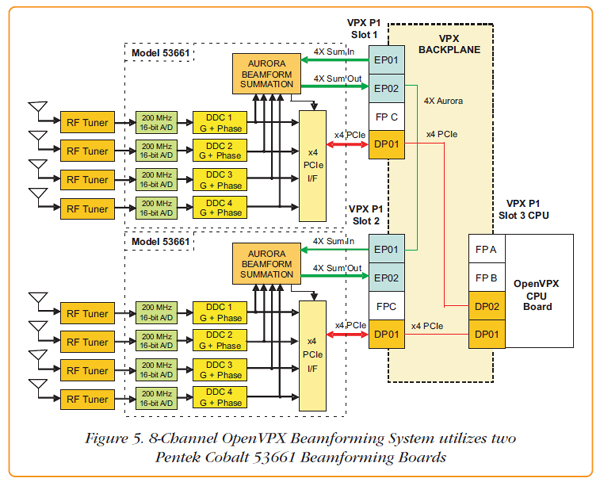 The 200 MHz 16-bit A/D converters digitize the IF signals and perform further frequency downconversion to baseband, with a DDC decimation of 128. This provides I+Q complex output samples with a bandwidth of about 1.25 MHz. Phase and gain coefficients for each channel are applied to steer the array for directionality. The CPU board in VPX slot 3 sends commands and coefficients across the backplane over two x4 PCIe links, or OpenVPX "fat pipes". The first four signal channels are processed in the upper left 53661 board in VPX slot 1, where the 4-channel beamformed sum is propagated through the 4X Aurora Sum Out link across the backplane to the 4X Aurora Sum In port on the second 53661 in slot 2. The 4-channel local summation from the second 53661 is added to the propagated sum from the first board to form the complete 8-channel sum. This final sum is sent across the x4 PCIe link to the CPU card in slot 3.
An additional display shows the beamformed pattern of the array. This display is formed by adjusting the phase shift of each of the eight channels to provide maximum sensitivity across arrival angles from -90 degree to +90 degree perpendicular to the plane of the array. The classic 7-lobe pattern for an ideal 8-element array for a signal arriving at 0 degree angle (directly in front of the array) is shown in Figure 7. Below the lobe pattern is a polar plot showing a single vector pointing to the computed angle of arrival. This is derived from identifying the lobe with the maximum response. 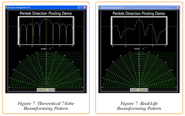 An actual plot of a real-life transmitter is shown in Figure 8 for a source directly in front of the display. In this case the perfect lobe pattern is affected by physical objects, reflections, cable length variations and minor differences in the antennas. Nevertheless, the directional information is computed quite well. As the signal source is moved left and right in front of the array, the peak lobe moves with it, changing the computed angle of arrival. This demo system is available online at Pentek, click here. If you are interested in viewing a live demonstration, please let us know of your interest by, clicking here. | ||||||
| CONNECT ON SOCIAL: |
|
|
|
|